- 您现在的位置:买卖IC网 > Sheet目录2005 > LTC2229IUH#PBF (Linear Technology)IC ADC 12-BIT 80MSPS 3V 32-QFN
LTC2229
17
2229fa
APPLICATIO S I FOR ATIO
WU
UU
DIGITAL OUTPUTS
Table 1 shows the relationship between the analog input
voltage, the digital data bits and the overflow bit.
As with all high speed/high resolution converters, the
digital output loading can affect the performance. The
digital outputs of the LTC2229 should drive a minimal
capacitive load to avoid possible interaction between the
digital outputs and sensitive input circuitry. The output
should be buffered with a device such as an ALVCH16373
CMOS latch. For full speed operation the capacitive load
should be kept under 10pF.
Lower OVDD voltages will also help reduce interference
from the digital outputs.
Data Format
Using the MODE pin, the LTC2229 parallel digital output
can be selected for offset binary or 2’s complement
format. Connecting MODE to GND or 1/3VDD selects offset
binary output format. Connecting MODE to
2/3VDD or VDD selects 2’s complement output format.
An external resistor divider can be used to set the 1/3VDD
or 2/3VDD logic values. Table 2 shows the logic states for
the MODE pin.
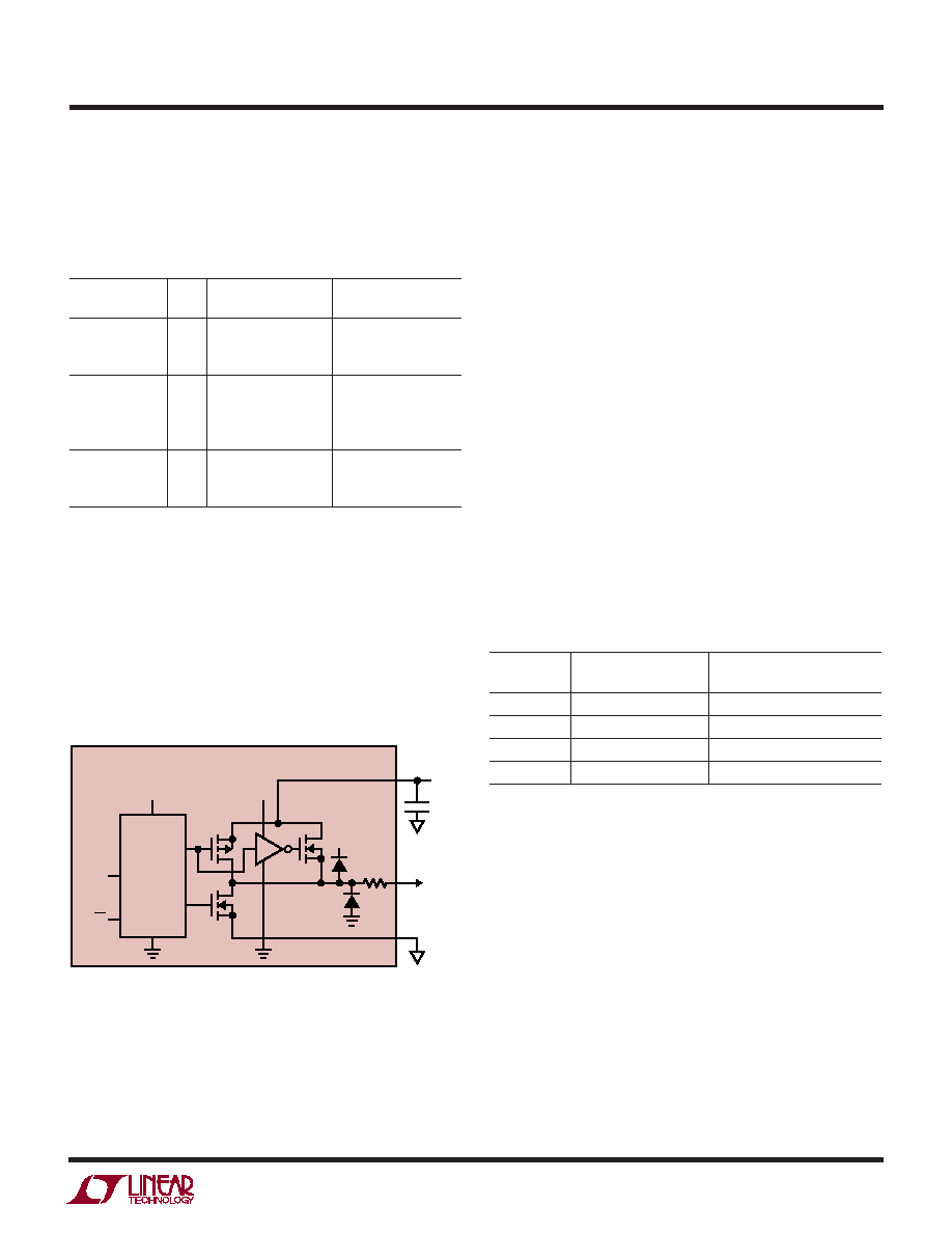
Figure 14. Digital Output Buffer
Table 1. Output Codes vs Input Voltage
AIN+ – AIN–
D11 – D0
(2V Range)
OF
(Offset Binary)
(2’s Complement)
>+1.000000V
1
1111 1111 1111
0111 1111 1111
+0.999512V
0
1111 1111 1111
0111 1111 1111
+0.999024V
0
1111 1111 1110
0111 1111 1110
+0.000488V
0
1000 0000 0001
0000 0000 0001
0.000000V
0
1000 0000 0000
0000 0000 0000
–0.000488V
0
0111 1111 1111
1111 1111 1111
–0.000976V
0
0111 1111 1110
1111 1111 1110
–0.999512V
0
0000 0000 0001
1000 0000 0001
–1.000000V
0
0000 0000 0000
1000 0000 0000
<–1.000000V
1
0000 0000 0000
1000 0000 0000
Digital Output Buffers
Figure 14 shows an equivalent circuit for a single output
buffer. Each buffer is powered by OVDD and OGND, iso-
lated from the ADC power and ground. The additional
N-channel transistor in the output driver allows operation
down to low voltages. The internal resistor in series with
the output makes the output appear as 50
to external
circuitry and may eliminate the need for external damping
resistors.
Table 2. MODE Pin Function
Clock Duty
MODE Pin
Output Format
Cycle Stablizer
0
Offset Binary
Off
1/3VDD
Offset Binary
On
2/3VDD
2’s Complement
On
VDD
2’s Complement
Off
LTC2229
2229 F12
OVDD
VDD
0.1
F
43
TYPICAL
DATA
OUTPUT
OGND
OVDD
0.5V
TO 3.6V
PREDRIVER
LOGIC
DATA
FROM
LATCH
OE
Overflow Bit
When OF outputs a logic high the converter is either
overranged or underranged.
发布紧急采购,3分钟左右您将得到回复。
相关PDF资料
LTC2231IUP#TRPBF
IC ADC 10BIT 135MSPS 64-QFN
LTC2233CUK#TRPBF
IC ADC 10BIT 80MSPS SAMPL 48QFN
LTC2234IUK#TRPBF
IC ADC 10BIT 135MSPS SAMPL 48QFN
LTC2237IUH#TRPBF
IC ADC 10BIT 40MSPS 3V 32-QFN
LTC2239CUH#PBF
IC ADC 10-BIT 80MSPS 3V 32-QFN
LTC2240CUP-12#PBF
IC ADC 12BIT 170MSPS 64-QFN
LTC2240IUP-10#PBF
IC ADC 10BIT 170MSPS 64-QFN
LTC2241IUP-10#PBF
IC ADC 10BIT 210MSPS 64-QFN
相关代理商/技术参数
LTC2229IUH#PBF
制造商:Linear Technology 功能描述:A/D Converter (A-D) IC
LTC2229IUH#TRPBF
功能描述:IC ADC 12BIT 80MSPS 3V 32-QFN RoHS:是 类别:集成电路 (IC) >> 数据采集 - 模数转换器 系列:- 标准包装:1 系列:- 位数:14 采样率(每秒):83k 数据接口:串行,并联 转换器数目:1 功率耗散(最大):95mW 电压电源:双 ± 工作温度:0°C ~ 70°C 安装类型:通孔 封装/外壳:28-DIP(0.600",15.24mm) 供应商设备封装:28-PDIP 包装:管件 输入数目和类型:1 个单端,双极
LTC222CJ
制造商:LINER 制造商全称:Linear Technology 功能描述:Micropower, Low Charge Injection, Quad CMOS Analog Switches with Data Latches
LTC222CN
功能描述:IC SWITCH QUAD SPST 16DIP RoHS:否 类别:集成电路 (IC) >> 接口 - 模拟开关,多路复用器,多路分解器 系列:- 标准包装:1,000 系列:- 功能:多路复用器 电路:1 x 4:1 导通状态电阻:- 电压电源:双电源 电压 - 电源,单路/双路(±):±5V 电流 - 电源:7mA 工作温度:-40°C ~ 85°C 安装类型:表面贴装 封装/外壳:16-SOIC(0.154",3.90mm 宽) 供应商设备封装:16-SOIC 包装:带卷 (TR)
LTC222CN#PBF
功能描述:IC SWITCH QUAD SPST 16DIP RoHS:是 类别:集成电路 (IC) >> 接口 - 模拟开关,多路复用器,多路分解器 系列:- 标准包装:48 系列:- 功能:开关 电路:4 x SPST - NO 导通状态电阻:100 欧姆 电压电源:单/双电源 电压 - 电源,单路/双路(±):2 V ~ 12 V,±2 V ~ 6 V 电流 - 电源:50nA 工作温度:-40°C ~ 85°C 安装类型:表面贴装 封装/外壳:16-SOIC(0.154",3.90mm 宽) 供应商设备封装:16-SOIC 包装:管件
LTC222CS
功能描述:IC SWITCH QUAD SPST 16SOIC RoHS:否 类别:集成电路 (IC) >> 接口 - 模拟开关,多路复用器,多路分解器 系列:- 标准包装:1,000 系列:- 功能:多路复用器 电路:1 x 4:1 导通状态电阻:- 电压电源:双电源 电压 - 电源,单路/双路(±):±5V 电流 - 电源:7mA 工作温度:-40°C ~ 85°C 安装类型:表面贴装 封装/外壳:16-SOIC(0.154",3.90mm 宽) 供应商设备封装:16-SOIC 包装:带卷 (TR)
LTC222CS#PBF
功能描述:IC SWITCH QUAD SPST 16SOIC RoHS:是 类别:集成电路 (IC) >> 接口 - 模拟开关,多路复用器,多路分解器 系列:- 标准包装:1,000 系列:- 功能:多路复用器 电路:1 x 4:1 导通状态电阻:- 电压电源:双电源 电压 - 电源,单路/双路(±):±5V 电流 - 电源:7mA 工作温度:-40°C ~ 85°C 安装类型:表面贴装 封装/外壳:16-SOIC(0.154",3.90mm 宽) 供应商设备封装:16-SOIC 包装:带卷 (TR)
LTC222CS#TR
功能描述:IC SWITCH QUAD SPST 16SOIC RoHS:否 类别:集成电路 (IC) >> 接口 - 模拟开关,多路复用器,多路分解器 系列:- 标准包装:1,000 系列:- 功能:多路复用器 电路:1 x 4:1 导通状态电阻:- 电压电源:双电源 电压 - 电源,单路/双路(±):±5V 电流 - 电源:7mA 工作温度:-40°C ~ 85°C 安装类型:表面贴装 封装/外壳:16-SOIC(0.154",3.90mm 宽) 供应商设备封装:16-SOIC 包装:带卷 (TR)